


Researchers at Huazhong University of Science and Technology have developed a comprehensive femtosecond laser-acoustic modeling and simulation framework to advance nondestructive testing (NDT) of metal nanofilms. This study, titled “Femtosecond Laser-Acoustic Modeling and Simulation for AlCu Nanofilm Nondestructive Testing,” presents a significant advancement in photoacoustic detection technology—a technique vital for assessing the thickness, integrity, and defects in nanostructured materials used in electronics, optics, and material science.
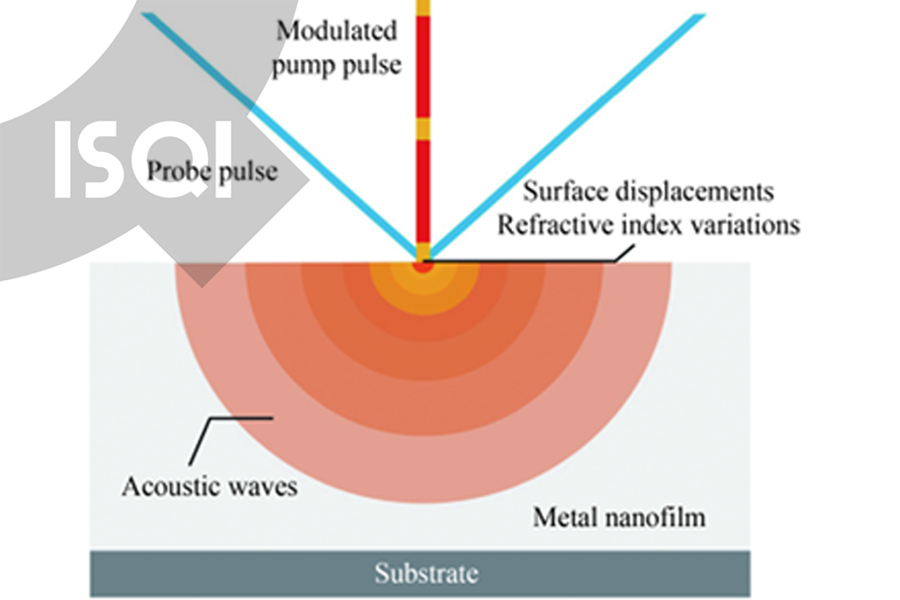
The research team combined the two-temperature model, which distinguishes between electron and lattice temperatures, with an acoustic wave generation and detection model. This integration provides a holistic understanding of laser-induced acoustic dynamics in nanofilms. The simulation model, developed using finite difference and finite element methods, visualizes the complete ultrafast laser-material interaction process during femtosecond photoacoustic testing of AlCu nanofilms. It enables precise calculations of temperature fields, stress, and strain distributions, while also determining the damage threshold of the laser for AlCu materials.
By systematically varying key parameters—laser fluence, pulse duration, and wavelength—the team demonstrated how these factors influence detection performance. Experiments conducted on 500 nm-thick AlCu nanofilms validated the numerical predictions, showing excellent agreement between simulation and experiment. This research offers critical insights into optimizing laser parameters for improved photoacoustic signal quality and detection accuracy. The developed model provides a scientific foundation that eliminates the need for trial-and-error parameter tuning, thus improving efficiency, repeatability, and reliability in nanoscale nondestructive testing.
By bridging the gap between laser physics, thermal dynamics, and acoustic signal modeling, the study represents an important step toward next-generation NDT technologies capable of detecting minute defects and variations in advanced thin-film materials. The findings have significant engineering and industrial implications, particularly in fields where precision and reliability are critical—such as semiconductor manufacturing, microelectronics, and advanced materials research.